At Vanguard Products Corporation, we are a global supplier of a wide selection of standard EMI/RFI shielding gaskets and conductive gaskets. These products are available in sizes ranging from 0.010 to 3 inches in cross-section and are highly customizable to meet the specific needs of our customers. Our finishing services include pressure sensitive adhesive (PSA) application, bonding, cutting, and additional secondary operations.
The Thermal Challenge
The proliferation of 5G systems, the increasing processing speeds and power of chips in conjunction with the inclusion of many transmitting and receiving antennas within electronics systems present numerous challenges to the mechanical, EMI, electrical, and antenna engineers. Coupled with this are the challenges of dealing with these issues while shrinking board sizes and packaging and reducing power consumption throughout the system.
Newer chips coming out on the market have extensive processing capabilities that are dependent upon controlling their temperature rise. When temperatures rise above certain thresholds, they are designed to “self-throttle” by reducing processing speeds and functions until their temperatures drop below the defined threshold. This limits the overall performance of the system.
Further complicating the matter is that often-times in mobile applications, these chips are placed in close proximity to transmitting and receiving antennas. As these high speed chips can emit a high level of EMI especially in areas directly around the chip, it becomes necessary to control the EMI emitting from the chips so that the noise floor within the system can be decreased, allowing for the antenna system to perform optimally (A term called “desense performance” within the antenna industry.)
Current designs require the elimination of circulating fans for concerns over enclosure size, weight, and battery life. As such, there have been numerous developments and improvements in passive thermal management systems for these electronics. Heat sinks, thermal spreaders, and heat pipes have been shrunken in size and improved in thermal efficiency to accommodate their inclusion into these systems. The main issue with these new approaches is that for them to be most efficient, they have to be in very close proximity to the thermally generating source (ie. the chip itself), and be in intimate contact with the heat source along with the heat removal apparatus.
Thermal Interface Materials (TIM) have been developed to allow for this. These materials are typically some type of compressible material with a filler that allows for an efficient transfer of energy from one interface to another. These materials operate best when the number of thermal interfaces are reduced (to reduce “thermal capacitance) and when thickness is minimized while subjected to the highest compressive force possible.
Traditional Approaches
The following figure is a schematic for the most commonly used approaches:
In this approach, an EMI shielding can is placed around the chip/component coupling with the board ground plane. On the heat sink/heat pipe side, the can either has an opening over which a copper tape is placed, or it is closed. The chip is coupled with a TIM material to the can/copper tape, and a piece of TIM is also placed on top of the copper tape/can to thermally couple the chip to the heat removal device (ie. heat sink, heat pipe).
Disadvantages:
- The complete package is relatively thick, causing the overall electronics package to grow and the TIM efficiency to decrease
- There are a minimum of 4 thermal interfaces between the hot component and the thermal sink, increasing the “thermal capacitance” at each interface, and reducing the efficiency of the TIM material
- The desense/EMI shielding is marginal
Results:
- Increased chip throttling frequency resulting in chip underperformance
- Decreased chip life
- Decreased antenna sensitivity
- Less EMI shielding margin
- Increased package size
Improved Integrated Approach
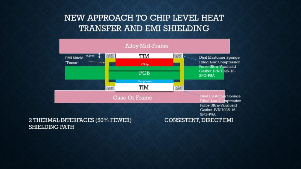
The following figure is a schematic for the improved integrated approach:
In this approach, the shield can or fence is reduced in height to align with the top of the chip/component.
A thin EMI gasket frame is installed around the opening and a TIM material is placed directly on top of the chip/component coupled to the thermal removal apparatus as shown below:


